
Friday, 16 January, 2026г.


Где искать: по сайтам Запорожской области, статьи, видео ролики
пример: покупка автомобиля в Запорожье
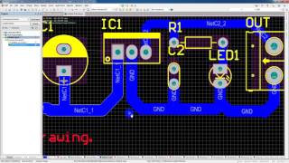
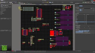
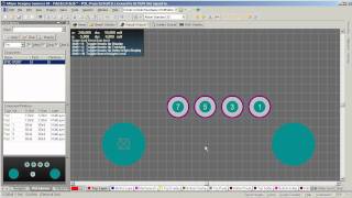
Altium Designer Tutorial 1: Schematic capture and PCB layout - Part2 ( Placement and Routing )
 У вашего броузера проблема в совместимости с HTML5
I hope it was useful for you! :)
In this first tutorial you will learn how to make a new project on Altium Designer, How to deal with components and to make your first Schematic file and make your first PCB .
Subscribe to our channel and if you have any questions don't hesitate sending your question below ! :)
--- Embedded Systems Tutorials---
Похожие видео
Мой аккаунт